Language
Opening Doors to Diversity in AI Chips
Release Date:2024-05-16
By Gao Zhenzhong
In 1956, at the Summer Seminar of Dartmouth College in the United States, scientists like McCarty and Minsky first proposed the concept of AI. Over the past 60 years, AI has undergone extensive development and exploration. By 2015, AI surpassed human visual recognition precision and entered large-scale commercial use in video applications. In 2022, ChatGPT emerged as a groundbreaking product, propelling the adoption of AI models in industrial applications.
As a crucial cornerstone of AI development, AI chips have undergone two major phases. Before 2012, AI research and applications primarily relied on CPUs. In 2012, Alex Krizhevsky from the University of Toronto pioneered the use of GPUs in AI, achieving a groundbreaking victory in the ImageNet competition using only four NVIDIA Geforce GTX 580s. This event astonished academia and opened the door to diversity in AI chips.
Key Requirements
AI chips can be divided into training and inference chips. Training involves providing a large amount of labeled or unlabeled data to adjust mode parameters through optimization algorithms, so that the model can learn related modes and laws from the data. Inference refers to applying a trained model to real-world scenarios for prediction, classification, or decision-making.
The key requirement of training chips is to enhance AI computing power and reduce model training duration. With the rise of AI models, their numbers and scales have exponentially increased within a few months. The emergence of 10-billion-level AI models and the birth of trillion-parameter AI models have intensified the demand for computing power during training, surpassing the pace of Moore’s Law for chip processing. As a result, the training time of AI models have consistently extended. For instance, OpenAI’s GPT-3 model with 175 billion parameters required approximately 1,024 A100 GPUs for a single run in 2022, while the GPT-4 model with 1.8 trillion parameters demanded about 25,000 A100 GPUs for a single run in 2023. Comparatively, the training time for GPT-4 nearly doubled that of GPT-3.
The requirements of inference chips vary based on service scenarios. For instance, in online Q&A scenarios, the computing power of AI chips needs to match reading speeds (250 words per minute, maximum 1,000 words). In 5GC scenarios, voice codec and image processing capabilities are necessary additions to AI computing power.
Deployment Location
AI chips are deployed primarily on the cloud and terminal sides. The cloud side refers to a cloud data center, while the terminal side refers to devices like mobile phones or PCs that can be accessed or used locally by individuals.
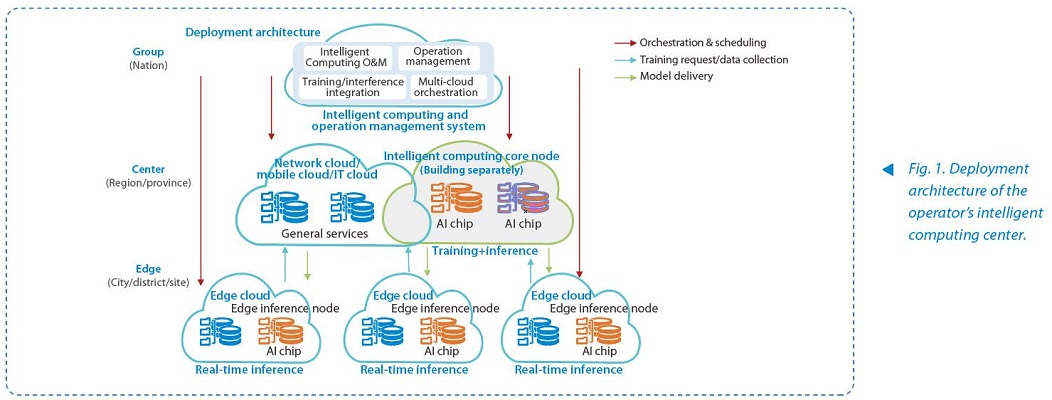
Taking the operator’s intelligent computing center as example, cloud data centers consist of group nodes, central nodes, and edge nodes (Fig. 1). Group nodes manage intelligent operations, central nodes handle training and non-real-time inference, while edge nodes and edge clouds are combined for real-time inference.
The terminal-side AI, with security, independence, low latency, and high reliability, efficiently handles diverse AI inference tasks. At present, multiple AI models have launched “miniaturization-based” and “scenario-based” versions, providing a basis for operation at the terminal side.
Technology Paths
The two leading AI chip technology paths are represented by the general parallel-computing architecture, exemplified by GPU, and the dedicated custom architecture tailored for accelerating AI tasks.
GPU is originally designed for graphic rendering, which involves extensive repetitive computing tasks. To meet the large-scale and parallel feature of AI operations, GPU chips deploy thousands of image computing cores capable of processing multiple tasks simultaneously.
Unlike GPUs, AI-dedicated chips are processors designed specifically for AI operations, utilizing AI-dedicated cores inside. They sacrifice video rendering and high-performance computing capabilities for advantages in power consumption and size. However, due to their dedicated and customized design, they have longer development periods and lack the universality and programmability of GPUs, resulting in many AI-dedicated chips being less powerful.
Looking into Future
The reality of trillion-parameter models is here, and even larger models may emerge soon. As the scale of models grows, both GPU and AI-dedicated chips face bottlenecks in performance and power consumption, resulting in the expansion of cloud data centers and the need for liquid cooling to manage heat dissipation. Additionally, devices at the terminal side like AI mobile phones and AI PCs are impacted by power consumption issues, affecting user experience. To solve these problems, the next-generation AI chip design focuses on the following directions:
- In computing architecture, the introduction of in-memory computing aims to reduce power consumption. Currently, mainstream GPUs and dedicated AI chips use the Von Neumann architecture, which separates computing from storage. However, 60% to 90% of chip energy is consumed during data migration. The in-memory computing architecture fully integrates memory and computing, avoiding data migration and greatly reducing power consumption.
- On the chip implementation layer, Chiplet and 3D stacking technologies are used to improve chip yield and performance. Chiplet divides a chip into multiple dies with specific functions (such as computing and storage), selecting the most suitable semiconductor process for each die to optimize yield. The dies are interconnected through a high-speed bus, and finally integrated and encapsulated into a single chip. 3D stacking expands chips from two-dimensional to three-dimensional, increasing the number of dies vertically, and improving chip performance while maintaining the original encapsulation size.
Related Articles